Wir verwenden Cookies und Analyse-Tools, um die Nutzerfreundlichkeit der Internet-Seite zu verbessern und für Marketingzwecke. Wenn Sie fortfahren, diese Seite zu verwenden, nehmen wir an, dass Sie damit einverstanden sind. Zur Datenschutzerklärung.
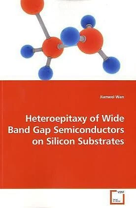
Heteroepitaxy of Wide Band Gap Semiconductors on Silicon Substrates
Details
The wide band gap semiconductors SiC and GaN have shown great potential for use in high-temperature, high-power and high-frequency electronic devices as well as short-wavelength optical devices. However, the lack of large-area and low-cost substrates hindered their development seriously. Thus, the heteroepitaxy of SiC and GaN on silicon substrates is highly desirable for the Si-based electronic industry. In this study, we investigated the epitaxy of 3C-SiC and hexagonal GaN on silicon substrates and related devices. High quality 3C-SiC epilayers were deposited with trimethylsilane and silane/propane precursors, respectively. Inversion- mode n-channel 3C-SiC MOSFET devices with high channel mobility have been successfully fabricated. For GaN growth, AlGaN/GaN heterostructures were grown on 100 mm diameter Si(111) substrates without cracking using a high-temperature AlN buffer layer and a 3C-SiC buffer layer. In addition, the growth of hexagonal GaN on Si(100) substrates was demonstrated for the first time using a sputtered AlN buffer layer followed by a MOCVD grown AlN buffer layer.
Autorentext
Jianwei Wan has been working for Dow Corning Corporation (Midland, Michigan) in the field of SiC epitaxy after receiving his Ph.D. degree in Electrical Engineering from Purdue University (West Lafayette, Indiana) in 2002. He also holds a B.S. degree and a M.S. degree in Physics from Tsinghua University, Beijing, China.
Weitere Informationen
- Allgemeine Informationen
- GTIN 09783639189254
- Anzahl Seiten 132
- Genre Wärme- und Energietechnik
- Herausgeber VDM Verlag
- Gewicht 213g
- Größe H220mm x B150mm x T8mm
- Jahr 2009
- EAN 9783639189254
- Format Kartonierter Einband (Kt)
- ISBN 978-3-639-18925-4
- Titel Heteroepitaxy of Wide Band Gap Semiconductors on Silicon Substrates
- Autor Jianwei Wan
- Sprache Englisch


